# Categories: general
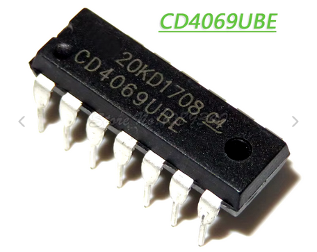
CD4069UBE Hex Inverter CMOS DIP-14
SEK12.00
Description
The CD4069UBE is a hex inverter IC from the CD4000 CMOS logic family, containing six independent NOT gates in a DIP-14 package. Supply voltage 3–18V. Suitable for logic inversion, oscillator and signal conditioning circuits.
Details
1 unit supplied in a ziplock bag with protective foam for pins